


Analog Devices Inc. ADRF5545A RF Front-End Multichip Module
Analog Devices Inc. ADRF5545A Dual-Channel RF Front-End Multichip Module is designed for time-division duplexing (TDD) applications that operate from 2.4GHz to 4.2GHz. The ADRF5545A is configured in dual channels with a cascading two-stage low noise amplifier (LNA) and a high-power silicon single-pole, double-throw (SPDT) switch.
In high gain mode, the cascaded two-stage LNA and switch offer a low noise figure (NF) of 1.45dB and a high gain of 32dB at 3.6GHz with an output third-order intercept point (OIP3) of 32dBm (typical). In low gain mode, one stage of the two-stage LNA is in bypass, providing 16dB of gain at a lower current of 36mA. In power-down mode, the LNAs are turned off and the device draws 12mA.
In transmit operation, when RF inputs are connected to a termination pin (TERM-ChA or TERM-ChB), the switch provides a low insertion loss of 0.65dB. The device handles long-term evolution (LTE) average power [9dB peak to average ratio (PAR)] of 40dBm for full lifetime operation and 43dBm for single event (<10s) LNA protection operation
Features
- Integrated dual-channel RF front end
- 2-stage LNA and high power SPDT switch
- On-chip bias and matching
- Single supply operation
- Gain at 3.6GHz
- 32dB typical high gain mode
- 16dB typical low gain mode
- Low noise figure at 3.6GHz
- 1.45dB typical high gain mode
- 1.45dB typical low gain mode
- High isolation
- RXOUT-CHA and RXOUT-CHB: 47dB typical
- TERM-CHA and TERM-CHB: 52dB typical
- Low 0.65dB typical insertion loss at 3.6GHz
- High power handling at TCASE = +105°C
- Full lifetime: 40dBm LTE average power (9dB PAR)
- Single event (<10s operation): 43dBm LTE average power (9dB PAR)
- 32dBm typical high OIP3
- Power-down mode and low gain mode for LNA
- Low supply current at 5V
- 86mA typical high gain mode
- 36mA typical low gain mode
- 12mA typical power-down mode
- Positive logic control
- 6mm×6mm, 40-lead LFCSP package
Applications
- Wireless infrastructure
- TDD massive multiple input/output and active antenna systems
- TDD-based communication systems
Functional Block Diagram

Technical Articles
- 5G Technology Devices for an O-RAN Wireless Solution
Discover a platform that meets the required RF characteristics, cost, and power budgets required to deploy a low-cost, high-performance O-RAN platform.
Development Tools
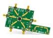
Analog Devices Inc. ADRF5545A-EVALZ Evaluation Board
Dinisenyo upang makatulong na suriin ang mga tampok at pagganap ng ADRF5545A, isang integrated na RF front end.
Associated Products
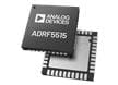
Analog Devices Inc. ADRF5515 Receiver Front-End
A dual-ch, integrated RF, front-end, multichip module designed for TDD applications.