Infineon Technologies OptiMOS™ 7 80V Automotive Power MOSFETs
Infineon Technologies OptiMOS™ 7 80V Automotive Power MOSFETs are built with Infineon’s leading-edge, power semiconductor technology. These MOSFETs are designed specifically for the high performance, quality, and robustness needed for demanding automotive applications. The OptiMOS™ 7 80V MOSFETs operate with a ±20VGS gate source voltage and a temperature range of -55°C to 175°C. These MOSFETs are offered in top-side cooled SSO10T 5x7mm2 SMD package. The SSO10T package helps users achieve advancements in cooling and power density. The 80V power MOSFETs are MSL-1 rated, RoHS compliant, and 100% avalanche tested. These power MOSFETs are ideal for general automotive applications.Features
- Direct cooling path to ECU housing
- Virtually no heat flows into the PCB
- Industry’s largest exposed pad area
- Freedom to route traces under the package
- Can mount parts on the back side of the PCB
- Leading edge on-resistance, RDS(on)
- Fast switching times (turn on/off)
- Tight threshold voltage, VGS(th) range
- Extended qualification beyond AEC-Q101
- Enhanced electrical testing
- Package is listed with JEDEC
- Enables excellent thermal management
- 20% to 50% improved thermal impedance
- 20% to 50% improved thermal resistance
- Helps reduce ECU volume or PCB area
- Helps reduce PCB cost (area, Cu, and vias)
- Reduces PCB and system design effort
- Helps achieve the highest power density
- Reduces conduction losses
- Superior switching performance
- Well-suited for parallel placement
- Quality and robustness for automotive
- Potential for a second source supplier
Applications
- Automotive:
- 48V Electric Power Steering (EPS)
- LED front lighting
- DC-AC inverters
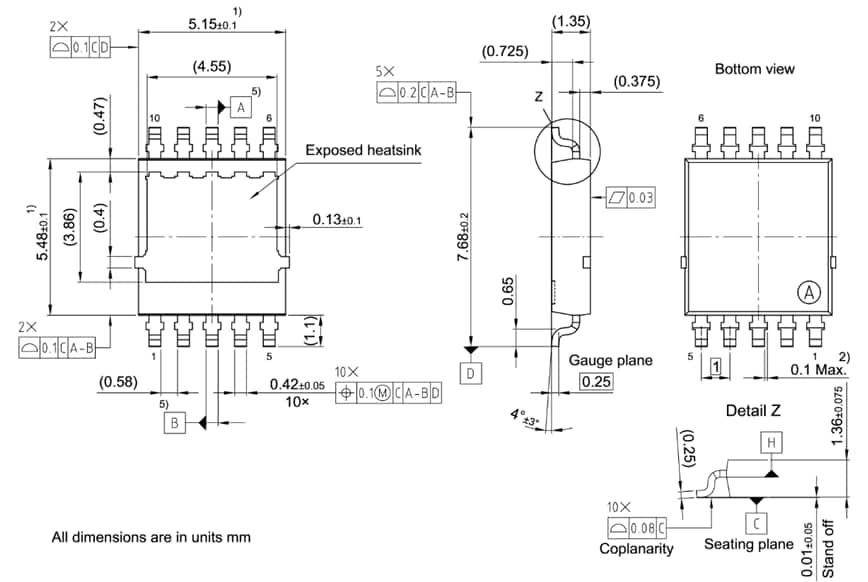
Dimensions

View Results ( 13 ) Page
| Numero ng Piyesa | Datasheet | Tagal ng Pagbagsak | Id - Continuous Drain Current | Package / Case | Pd - Power Dissipation | Qg - Gate Charge | Rds On - Drain-Source Resistance | Tagal ng Pagtaas | Vds - Drain-Source Breakdown Voltage | Vgs - Gate-Source Voltage | Vgs th - Gate-Source Threshold Voltage |
|---|---|---|---|---|---|---|---|---|---|---|---|
| IAUZN08S7N046ATMA1 |  |
7 ns | 99 A | PG-TDSON-8 | 94 W | 27.2 nC | 4.6 mOhms | 3.7 ns | 80 V | 20 V | 3.2 V |
| IAUCN08S7L018ATMA1 |  |
25 ns | 210 A | PG-TDSON-8 | 169 W | 79.9 nC | 1.8 mOhms | 11 ns | 80 V | 20 V | 2 V |
| IAUCN08S7L024ATMA1 |  |
20 ns | 177 A | PG-TDSON-8 | 148 W | 65.2 nC | 2.4 mOhms | 9 ns | 80 V | 16 V | 2 V |
| IAUCN10S7L040ATMA1 |  |
14 ns | 130 A | PG-TDSON-8 | 118 W | 44.3 nC | 3.3 mOhms | 5.9 ns | 100 V | 16 V | 2 V |
| IAUZN10S7N078ATMA1 |  |
5 ns | 76 A | PG-TDSON-8 | 94 W | 22.2 nC | 7.8 mOhms | 3.6 ns | 100 V | 20 V | 3.2 V |
| IAUCN08S7L013ATMA1 |  |
35 ns | 293 A | PG-TDSON-8 | 219 W | 120 nC | 1.26 mOhms | 14 ns | 80 V | 20 V | 2 V |
| IAUCN08S7L033ATMA1 |  |
14 ns | 130 A | PG-TDSON-8 | 118 W | 44.3 nC | 3.3 mOhms | 5.9 ns | 80 V | 16 V | 2 V |
| IAUCN08S7N016TATMA1 |  |
20 ns | 262 A | PG-LHDSO-10-3 | 205 W | 83 nC | 1.63 mOhms | 18 ns | 80 V | 20 V | 3.2 V |
| IAUCN08S7N019TATMA1 |  |
17 ns | 223 A | PG-LHDSO-10-2 | 180 W | 68 nC | 1.94 mOhms | 16 ns | 80 V | 20 V | 3.2 V |
| IAUCN08S7N024TATMA1 |  |
16 ns | 186 A | PG-LHDSO-10-1 | 157 W | 54 nC | 2.44 mOhms | 16 ns | 80 V | 20 V | 3.2 V |
Inilathala: 2025-07-23
| Na-update: 2025-08-19


