


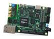
Altera DK-DEV-10M50C MAX 10 FPGA Development Board
Altera DK-DEV-10M50C MAX 10 FPGA development board evaluates the performance and features of the Altera MAX 10 device. The board may be programmed using the embedded USB-Blaster™ II or an optional JTAG 10-pin header.
The DK-DEV-10M50C features include two-gigabit ethernet ports, mini-USB 2.0 UART, HDMI, a universal high-speed mezzanine card (HSMC) connector, and two 12-pin Digilent Pmod™ compatible connectors.
Features
- MAX 10 FPGA (10M50D, dual supply, F484 package)
- MAX II CPLD - EPM1270M256C4N (on-board USB-Blaster II)
- Programming and configuration:
- Embedded USB-Blaster II (JTAG)
- Optional JTAG direct via a 10-pin header
- Memory devices:
- 64M x16 1Gb DDR3 SDRAM with soft memory controller
- 128M x8 1Gb DDR3 SDRAM with soft memory controller
- 512Mb quad serial peripheral interface (quad SPI) Flash
- Communication ports:
- Two gigabit Ethernet (GbE) RJ-45 ports
- Ethernet Port A (bottom)
- Ethernet Port B (top)
- One mini-USB2.0 UART
- One high-definition multimedia interface (HDMI) video output
- One universal high-speed mezzanine card (HSMC) connector
- Two 12-pin Digilent Pmod compatible connectors
- Analog:
- Two MAX 10 FPGA Analog-to-Digital Converter (ADC) SMA inputs
- Two x10 ADC header
- Potentiometer input to ADC
- One external 16-bit Digital-to-Analog Converter (DAC) device with SMA output
- Clocking:
- 25MHz single-ended, external oscillator clock source
- Silicon Labs clock generator with programmable frequency GUI
Kit Contents
- Free Quartus® II Web Edition design software (download software and license from website)
- Mini-USB cable for on-board USB-Blaster II
- 2A power supply and cord
- Complete documentation
- User manual, bill of materials, schematic, and board files
Front

Back

Related Products
Altera MAX® 10 FPGA Evaluation Boards
General-purpose development platforms for applications like industrial and automotive.
Design Software

Altera Quartus® Prime Design Software
Multi-platform design environment for all phases of FPGA and CPLD design.
Inilathala: 2019-08-27
| Na-update: 2025-04-22