NXP Semiconductors P3A1604UK Dual Supply Translating Transceiver
NXP Semiconductors P3A1604UK Dual Supply Translating Transceiver is a versatile 4-bit device designed for bidirectional voltage level translation with auto direction sensing. The NXP P3A1604UK IC supports a wide supply voltage range, with VCCA from 0.72V to 1.98V and VCCB from 1.62V to 3.63V, making it suitable for interfacing between different voltage nodes. The P3A1604UK is ideal for I3C, I2C, SMBus, and SPI applications, offering a maximum data rate of 40Mbps in push-pull mode. The robust design includes ESD protection exceeding 2000V (HBM) and 500V (CDM), and the IC operates reliably across a temperature range of -40°C to +125°C. This transceiver is perfect for mobile, industrial, and consumer applications, providing seamless integration and efficient voltage level translation.Features
- Auto direction sensing and bidirectional voltage level translation
- Wide supply voltage range
- 0.72V to 1.98V for VCCA
- 1.62V to 3.63V for VCCB
- No power-sequencing required
- Maximum data rate (DDR) per bit
- 6.8Mbit/s (3.4MHz) open-drain
- 40Mbit/s (20MHz) push-pull
- Supports I3C, I2C, SMBus, SPI, and UART interfaces
- Longer one-shot pulse for driving larger capacitive loads with reduced ringing and overshoot
- A-side and OE inputs accept voltages up to 1.98V
- B-side inputs accept voltages up to 3.63V
- Electrostatic Discharge (ESD) protection
- HBM exceeds 2000V per JESD22-A114E Class 2
- CDM exceeds 500V per JESD22-C101E
- 100mA I/O latch-up current, JESD 78
- WLCSP12 (SOT2063-4) package, 1.405mm x 1.055mm with a 0.35mm pitch
- -40°C to +125°C operating temperature range
Applications
- Mobile
- I3C, I2C, and SMBus
- SPI
- Servers
Specifications
- 10ns/V maximum input transition rise/fall rate
- 1μA maximum input leakage current
- 2μA to 3μA maximum OFF-state output current range
- 2pF typical input capacitance
- Typical I/O capacitance
- 7pF for A port
- 5.5pF for B port
- 3μs maximum enable time
- 0.4μs to 0.8μs disable time range
- 0.3ns maximum output skew time between channels
- 0.128Mbit/s to 40Mbit/s data rate range
- Thermal resistance
- 77.9°C/W junction-to-ambient
- 9.3°C/W junction-to-top characterization
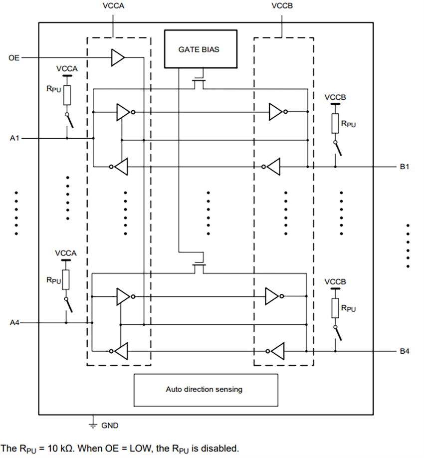
Block Diagram

Typical Application Circuit

Architecture

Inilathala: 2025-04-21
| Na-update: 2025-04-24


