


ROHM Semiconductor LAPIS ML610Q327/ML610Q338/ML610Q339 8-Bit MCUs
ROHM Semiconductor LAPIS ML610Q327/ML610Q338/ML610Q339 8-Bit Microcontrollers (MCUs) are high-performance 8-bit CMOS MCUs that integrate a wide variety of peripherals such as timer, PWM, UART, I2C bus interface, synchronous serial port, successive approximation type 10-bit A/D converter and voice output function. The nX-U8/100 CPU can execute instructions efficiently on a one-instruction-per-clock-pulse basis through parallel processing by the 3-stage pipelined architecture. The ROHM Semiconductor LAPIS ML610Q327 / ML610Q338 / ML610Q339 is also equipped with a flash memory that has achieved low voltage and low power consumption (at read) equivalent to mask ROM, so it is well suited to battery-driven applications such as alarm and portable devices. In addition, it has an on-chip debugging function, which allows software debugging/rewriting with the LSI mounted on the board.
Features
- CPU
- 8-bit RISC CPU (CPU name: nX-U8/100)
- Instruction system: 16-bit instructions
- Instruction set (transfer, arithmetic operations, comparison, logic operations, multiplication/division, bit manipulations, bit logic operations, jump, conditional jump, call return stack manipulations, arithmetic shift, and so on)
- On-chip debug function
- Minimum instruction execution time
- Approx 30.5μs (at 32.768kHz system clock)
- Approx 0.244μs (at 4.096MHz system clock) at VDD = 2.0V to 5.5V
- Approx 0.122μs (at 8.192MHz system clock) at VDD = 2.2V to 5.5V
- Internal memory
- Flash memory
- ML610Q327 - 192Kbyte (96K x 16bits) program area with a rewrite cycle of 100 times
- ML610Q338/ML610Q339 - 256Kbyte (128K×16bits) program area with a rewrite cycle of 100 times
- Data Flash memory of 2Kbyte (1K x 16 bits) with a rewrite cycle of 10,000 times
- Built into Back Ground Operation (BGO) function (CPU continues program processing while the data flash erase/write)
- Internal RAM is 4Kbyte (4K x 8 bits)
- Flash memory
- Interrupt controller
- One non-maskable interrupt source is one watchdog timer
- 29 maskable interrupt sources
- Internal source has 21 (Data Flash erase/write completion, SSIO0, SSIO1, UART0, UART1, I2C bus master/slave interface, Timer 0, Timer 1, Timer 2, Timer 3, PWM0, PWM1, PWM2, A/D converter, voice sound reproduction, speaker pin short detection, TBC128Hz, TBC32Hz, TBC16Hz, TBC2Hz)
- External source of 8 (P80, P81, P82, P83, P84, P85, P86, P87)
- Time base counter
- Low-speed time base counter x 1-channel
- High-speed time base counter x 1-channel
- Watchdog timer
- Generates a non-maskable interrupt upon the first overflow, and a system reset occurs upon the second
- Free running
- Overflow period of four types, selectable as 125ms, 500ms, 2s, and 8s at 32.768kHz
- Timer (8-bit x 4-ch (16-bit configuration available)
- PWM with a resolution of 16 bits x 3-ch
- Voice output function
- Voice synthesis method of HQ-ADPCM, 4-bit ADPCM2, non-linear 8-bit PCM, straight 8-bit PCM, and straight 16-bit PCM
- Sampling frequency of 6.4kHz, 8kHz, 10.7kHz, 12.8kHz, 16kHz, 21.3kHz, 25.6kHz, and 32kHz
- Successive approximation type A/D converter
- 10-bit A/D converter
- Input of 8-channels
- Conversion time of 24.4μs per channel at 4.096MHz VDD ≥ 2.2V
- Conversion time of 12.2μs per channel at 8.192MHz VDD ≥ 2.5V
- Continuous conversion/single conversion selectable
- Synchronous serial port (SSIO)
- 2-channel
- Master/slave selectable
- LSB first/MSB first selectable
- 8-bit length/16-bit length selectable
- UART
- Half-duplex x 2-ch (a full-duplex is also possible by using 2-channels)
- TXD/RXD
- Bit length, parity/no parity, odd parity/even parity, 1 stop bit/2 stop bits
- Positive logic/negative logic selectable
- Built-in baud rate generator
- I2C bus interface
- Master function (standard mode (100kbps) and Fast mode (400kbps))
- Slave function (standard mode (100kbps) and Fast mode (400kbps))
- General-purpose ports
- Output-only port x 6-channel (including secondary functions)
- Input/output port (including secondary functions)
- ML610Q327 26-channel
- ML610Q338 30-channel
- ML610Q339 42-channel
- Speaker amplifier (D-class) output power
- 1.0W (at 5.0V)/0.45W (at 3.0V)
- Disconnection detection circuit
- Speaker pin short detection circuit
- Reset
- Reset through the RESET_N pin
- Power-on reset generation when powered on
- Reset by the watchdog timer (WDT) overflow
- PLL oscillation stop detection reset
- Low-level detection (LLD) reset
- Clock
- Low-speed clock (built-in RC oscillation (32.768kHz)
- High-speed clock (built-in PLL oscillation (approx. 1.024MHz/2.048MHz/4.096MHz/8.192MHz)
- Power management
- STOP mode (stop of oscillation (operations of CPU and peripheral circuits are stopped))
- HALT mode (instruction execution by CPU is suspended (peripheral circuits are in operating states))
- Clock gear (the frequency of the high-speed system clock can be changed by software (1/2, 1/4, 1/8, or 1/16 of the oscillation clock))
- Block control function (operation of an intact functional block circuit is powered down (register, reset, and clock stop))
- Packages
- ML610Q327 48-pin TQFP (P-TQFP48-0707-0.50-ZK6)
- ML610Q338 52-pin TQFP (P-TQFP52-1010-0.65-ZK6)
- ML610Q339 64-pin TQFP (P-TQFP64-1010-0.50-ZK6)
- Guaranteed operating range
- −40°C to 85°C operating temperature
- VDD = 2.0V to 5.5V, SPVDD = 2.0V to 5.5V operating voltage
Applications
- Consumer electronics
- Internet of Things (IoT) devices
- Automotive electronics
- Industrial automation
- Toys and educational products
- Security systems
- Wearables
Block Diagrams


Related Development Tools

ROHM Semiconductor RB-D610Q327TB48 Reference Board
Development platform designed for the LAPIS ML610Q327 8-bit microcontroller.

ROHM Semiconductor RB-D610Q338TB52 Reference Board
Facilitates the evaluation and prototyping of the LAPIS ML610Q338 8-bit microcontroller.

ROHM Semiconductor RB-D610Q339TB64 Reference Board
Develops and tests applications using the ML610Q339 8-bit speech playback microcontroller.
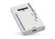
ROHM Semiconductor EASE1000 V2 On-chip Emulator
Debugger, flash writer, and emulator for ROHM / Lapis ML62Q1000, ML610Qx, and ML620Qx MCUs.
Inilathala: 2024-11-27
| Na-update: 2024-12-23