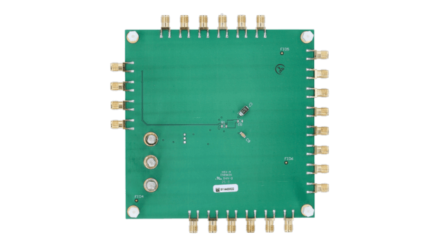
Texas Instruments CDCLVP111SEPEVM Evaluation Module
Texas Instruments CDCLVP111SEPEVM Evaluation Module offers a platform for evaluating the CDCLVP111-SEP clock buffer under various voltage and bias configurations. The CDCLVP111-SEP clock driver distributes one differential clock pair of LVPECL input (CLK0, CLK1) to ten pairs of differential LVPECL clock (Q0, Q9) outputs with minimum skew for clock distribution. The CDCLVP111-SEP is characterized for operation from –55°C to +125°C.The TI CDCLVP111SEPEVM Evaluation Module setup is effectively a breakout board that exposes the full functionality of the device, delivering flexible input and output biasing options.
Features
- Distributes one of two differential input clocks to 10 differential LVPECL output clocks
- Clock input selectable
- Low output skew
- Wide supply range
Applications
- Designed for driving 50Ω transmission lines
- High-performance clock distribution
- Communications payloads
- Radar imaging payload
- Command data handling
Overview - Front

Overview - Back

Inilathala: 2025-10-13
| Na-update: 2025-10-22


