


Texas Instruments SN74AVC8T245/SN74AVC8T245-Q1 Bus Transceiver
Texas Instruments SN74AVC8T245/SN74AVC8T245-Q1 Dual Supply Bus Transceiver is an 8-bit, non-inverting bus transceiver using two configurable power supply rails. The SN74AVC8T245/SN74AVC8T245-Q1 is optimized to operate with VCCA/VCCB set at 1.4V to 3.6V. The device is operational with VCCA and VCCB at a low level of 1.2V. The A port is designed to track VCCA, and the B port is designed to track VCCB. VCCA and VCCB accept any supply voltage from 1.2V to 3.6V. This feature allows universal bidirectional low-voltage translation between the 1.2V, 1.5V, 1.8V, 2.5V, and 3.3V voltage nodes.
The SN74AVC8T245/SN74AVC8T245-Q1 is designed for asynchronous communication between data buses. The device transmits data from the A bus to the B bus or from the B bus to the A bus. This feature depends on the logic level at the direction-control (DIR) input. The output-enable (OE) input can disable the outputs, effectively isolating the buses. The SN74AVC8T245/SN74AVC8T245-Q1 is designed so that VCCA supplies the control pins (DIR and OE).
The SN74AVC8T245/SN74AVC8T245-Q1 can be replaced later with a ’245 function and is compatible with a single-supply system with minimal printed circuit board redesign. This device is fully specified for partial power-down applications using Ioff. The Ioff circuitry prevents damaging current backflow through the device by disabling the outputs when powered down.
The VCC isolation feature allows both ports to be in the high-impedance state when either VCC input is at GND. To put the device into the high-impedance state during power down or power up, tie OE to VCC through a pullup resistor; the driver's current-sinking capability determines the minimum value of the resistor. The Texas Instruments SN74AVC8T245-Q1 devices are AEC-Q100 qualified for automotive applications.
Applications
- Latch-up performance exceeds 100mA per JESD 78, Class II
- ESD protection exceeds JESD 22
- 8000V human-body model (A114-A)
- 200V machine model (A115-A)
- 1000V charged-device model (C101)
- Control inputs VIH/VIL levels are referenced to the VCCA voltage
- VCC isolation feature (if either VCC input is at GND, all I/O ports are in the high-impedance state)
- Ioff supports partial power-down mode operation
- A fully configurable dual-rail design allows each port to operate over the full 1.4V to 3.6V power supply range
- I/Os are 4.6V tolerant
- Maximum data rates
- 170Mbps (VCCA < 1.8V or VCCB < 1.8V)
- 320Mbps (VCCA ≥ 1.8V and VCCB ≥ 1.8V)
Applications
- Personal electronic
- Industrial
- Enterprise
- Telecom
Additional Resources
- SN74AVC8T245 Datasheet
- SN74AVC8T245-Q1 Datasheet
- Application Note: Understanding Transient Drive Strength vs. DC Drive Strength in Level-Shifters
- Application Note: Overcoming Design Challenges - Implementing High Performance Interfaces
- Application Brief: Translate Voltages for RGMII
- Selection Guide: Voltage Translation Buying Guide
- Selection Guide: Logic Guide
- Application Note: Understanding and Interpreting Standard-Logic Data Sheets
- Application Note: Voltage Translation Between 3.3V, 2.5V, 1.8V, and 1.5V Logic Standards
- User Guide: LOGIC Pocket Data Book
Functional Block Diagram

Development Tools
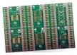
Texas Instruments 14-24-LOGIC-EVM Logic Evaluation Module (EVM)
Generic evaluation module developed to support any TI logic leaded device in a 14 to 24 pin count.
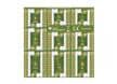
Texas Instruments 14-24-NL-LOGIC-EVM Logic Evaluation Module (EVM)
Supports any logic or translation device in a BQA, BQB, RGY (14-24 pin), RSV, RJW, or RHL package.
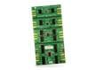
Texas Instruments AVCLVCDIRCNTRL-EVM Direction Evaluation Module
Offers support for 1, 2, 4, and 8-ch LVC and AVC family direction-controlled translation devices.
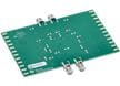
Texas Instruments TXV010xEVM Evaluation Module (EVM)
Easy-to-use platform for evaluating the performance and functionality of the TXV010x devices.

Texas Instruments EVMK2GX/EVMK2GXS 1GHz Evaluation Module (EVM)
Enables developers to immediately start evaluating the 66AK2Gx processor family.