


Texas Instruments SN74LXC1T45/SN74LXC145-Q1 Bus Transceiver
Texas Instruments SN74LXC1T45/SN74LXC145-Q1 Dual-Supply Bus Transceiver is a 1-bit, dual-supply non-inverting bidirectional voltage level translation device. The I/O pin A and control pin (DIR) are referenced to VCCA logic levels, and the I/O pin B is referenced to VCCB logic levels. The A pin on the Texas Instruments SN74LXC1T45/SN74LXC145-Q1 can accept I/O voltages ranging from 1.1V to 5.5V, while the B pin can accept I/O voltages from 1.1V to 5.5V. A high on DIR allows data transmission from A to B, and a low DIR allows data transmission from B to A. The SN74LXC145-Q1 devices are AEC-Q100 qualified for automotive applications.
Features
- A fully configurable dual-rail design allows each port to operate from 1.1V to 5.5V
- Robust, glitch-free power supply sequencing
- Up to 420Mbps support for 3.3V to 5.0V
- Schmitt-trigger inputs allow for slow or noisy inputs
- I/O’s with integrated dynamic pull-down resistors help reduce external component count
- Control inputs with integrated static pull-down resistors allow for floating control inputs
- High drive strength (up to 32mA at 5V)
- Low power consumption
- 3µA maximum (25°C)
- 6µA maximum (–40°C to 125°C)
- VCC isolation and VCC disconnect (Ioff-float) feature
- If either VCC supply is < 100mV or disconnected, all of the I/Os get pulled down and then become high-impedance
- Ioff supports partial-power-down mode operation
- Compatible with LVC family level shifters
- Control logic (DIR and OE) are referenced to VCCA
- Operating temperature from –40°C to +125°C
- Latch-up performance exceeds 100 mA per JESD 78, class II
- ESD protection exceeds JESD 22
- 4000V human-body model
- 1000V charged-device model
Applications
- Eliminate slow or noisy input signals
- Driving indicator LEDs or buzzers
- Debouncing a mechanical switch
- General purpose I/O level shifting
Datasheets
Functional Block Diagram

Related Development Tool
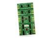
Texas Instruments AVCLVCDIRCNTRL-EVM Direction Evaluation Module
Offers support for 1, 2, 4, and 8-ch LVC and AVC family direction-controlled translation devices.
Inilathala: 2022-03-16
| Na-update: 2022-11-04