


Renesas Electronics RX651 & RX65N RX Microcontrollers
Renesas Electronics RX651 and RX65N RX Microcontrollers add four 64-pin MCUs to mainstream RX651 and RX65N MCUs that use the RXv2 Core CPU. The 64-pin MCUs enable security and flash functionality for industrial applications. Each Renesas MCU's Trusted Secure IP (TSIP) and Flash area protection provides root of trust device operation. The dual-bank flash feature (BGO and swap) makes the flash firmware update easier through secure network communication. The 64-pin package reduces the PCB footprint area for IoT edge applications.
Features
- 32-bit RXv2 CPU core
- 120MHz maximum operating frequency capable of 240 DMIPS in operation at 120MHz
- Single-precision 32-bit IEEE-754 floating-point
- Two types of multiply-and-accumulation unit (between memories and between registers)
- 32-bit multiplier (fastest instruction execution takes one CPU clock cycle)
- Divider (fastest instruction execution takes two CPU clock cycles)
- Fast interrupt
- CISC Harvard architecture with 5-stage pipeline
- Variable-length instructions - ultra-compact code
- Supports the memory protection unit (MPU)
- JTAG and FINE (one-line) debugging interfaces
- Low-power design and architecture
- 2.7V to 3.6V single-supply operation
- Low power consumption - supports all peripheral functions, drawing only 0.19mA/MHz (typical)
- RTC is capable of operation from a dedicated power supply.
- Four low-power modes
- On-chip code flash memory
- Supports versions with up to 2 Mbytes of ROM
- No wait cycles at up to 50MHz or when the ROM cache is hit, onewait state at up to 100MHz, two-wait state at above 100MHz
- User code is programmable by on-board or off-board programming.
- Programming/erasing as background operations (BGOs)
- A dual-bank structure allows exchanging the start-up bank.
- On-chip data flash memory
- 32Kbytes, reprogrammable up to 100,000 times
- Programming/erasing as background operations (BGOs)
- On-chip SRAM, no wait states
- 256/640Kbytes of SRAM (no wait states)
- 8Kbytes of standby RAM (backup on deep software standby)
- Data transfer
- 8-channel DMACAa
- 1-channel DTCb
- 2-channel EXDMAC
- 1-channel DMAC for the Ethernet controller
- Reset and supply management
- Power-on reset (POR)
- Low voltage detection (LVD) with voltage settings
- Clock functions
- External crystal resonator or internal PLL for operation at 8MHz to 24MHz
- Internal 240-kHz LOCO and HOCO selectable from 16MHz, 18MHz, and 20MHz
- 120kHz clock for the IWDTa
- Real-time clock
- Adjustment functions (30 seconds, leap year, and error)
- Real-time clock counting and binary counting modes are selectable
- Time capture function (for capturing times in response to event-signal input)
- Independent watchdog timer
- 120kHz (1/2 LOCO frequency) clock operation
- Useful functions for IEC60730 compliance
- Oscillation-stoppage detection, frequency measurement, CRCA, IWDTa, self-diagnostic function for the A/D converter, etc.
- Register write protection function can protect values in important registers against overwriting
- Various communications interfaces
- Ethernet MAC (1 channel)
- PHY layer (1 channel) for host/function or OTG controller (1 channel) with full-speed USB 2.0 transfer
- CAN (compliant with ISO11898-1), incorporating 32 mailboxes (up to 2 channels)
- SCIg and SCIh with multiple functionalities (up to 11 channels) Choose from among asynchronous mode, clock-synchronous mode, smart-card interface mode, simplified SPI, simplified I2C, and extended serial mode
- SCIi with 16-byte transmission and reception FIFOs (up to 2 channels)
- I2C bus interface for transfer at up to 1 Mbps (up to 3 channels)
- Four-wire QSPI (1 channel) in addition to RSPIc (3 channels)
- Parallel data capture unit (PDC) for the CMOS camera interface
- Graphic-LCD controller (GLCDC)
- 2D drawing engine (DRW2D)
- SD host interface (optional: 1 channel) with a 1- or 4-bit SD bus for use with SD memory or SDIO
- SD slave interface (optional: 1 channel) with a 1- or 4-bit SD bus for use with SD host interface
- MMCIF with 1-, 4-, or 8-bit transfer bus width
- External address space
- Buses for full-speed data transfer (60MHz max operating frequency)
- 8 CS areas
- 8-, 16-, or 32-bit bus space is selectable per area
- Independent SDRAM area (128 Mbytes)
- Up to 25 extended-function timers
- 16-bit TPUa, MTU3a
- 8-bit TMRa (4 channels), 16-bit CMT (4 channels), 32-bit CMTW (2 channels)
- 12-bit A/D converter
- Two 12-bit units (8 channels for unit 0; 21 channels for unit 1)
- Self-diagnosis, detection of analog input disconnection
- 2-channel 12-bit D/A converter
- Temperature sensor for measuring temperature within the chip
- Encryption functions (optional)
- AES (key lengths: 128, 192, and 256 bits)
- Trusted Secure IP (TSIP)
- Up to 136 pins for general I/O ports - 5V tolerance, open drain, input pull-up, switchable driving ability
- Operating temperature range
- D-version: –40°C to +85°C
- G-version: –40°C to +105°C
Block Diagram

Additional Resources
- Release Note: QE for Display[RX,RA] V3.2.0
- Migration Guide from the M16C to the RX: Timers
- Migration Guide from the M16C to the RX: Clocks
- Application Note: RX Dual Mode Usage Guide
- Technical Update: Decoupling Capacitance for Stabilizing the Internal Voltage
- Application Note: FS3000 Sample Software Manual
- Application Note: FS2012 Sample Software Manual
- Application Note: HS300x Sample Software
- Application Note: Sensor Software Combination Manual
- Application Note: RA Family, RX Family, RL78 Family
- Application Note: RX Family RX Driver Package
- Azure RTOS sample projects using e2 studio or IAR EW
- AES Library Firmware Application Note
- Firmware Update Module Application Note
- Reality AI Data Shipper Control Module Firmware Integration Technology
- Reality AI UART Communication Module Firmware Integration Technology
- Reality AI Control Modules Firmware Integration Technology
- Reality AI Data Acquisition Module (Data Collector / Data Shipper) – Sample Code
- RL78 FAMILY HARDWARE MANUAL GUIDE-ELECTRICAL CHARACTERISTICS EDITION
- ADC Migration Guide: H8SX/1668 to RX65N (Application Note)
- Application Note: HS400x Sample Software Manual
Related Kits

Renesas Electronics RAA2S425XKIT Evaluation Kit
Demonstration and development platform for the RAA2S425x Automotive Sensor Signal Conditioners.
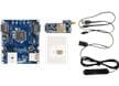
Renesas Electronics CK-RX65N V2 Cloud Kit
Enables secure connection to the cloud and explores the features of the Renesas RX65N MCUs.
Related Solutions

Renesas Electronics Electronic Lock with Fingerprint Identification
Features an RX130 MCU, low power design, and shock-sensor monitoring for tampering and break-ins.

Renesas Electronics Smart Locks with Super Low Power Wi-Fi® and BLE
Aim for a rapidly growing segment of the smart home and building automation industries.
Related MCUs
Renesas Electronics RX 32-bit Microcontrollers
Features high-performance RXv1/RXv2 CPU core with good operation performance and power efficiency.
Inilathala: 2019-07-30
| Na-update: 2023-12-12